
A study published in “Advanced Materials” reveals the thermal transport properties of ultrathin crystals of molybdenum diselenide, a two-dimensional material of the transition metal dichalcogenide (TMD) family. Outperforming silicon, TMD materials prove to be outstanding candidates for electronic and optoelectronic applications, such as flexible and wearable devices. This research, which involved researchers belonging to four ICN2 groups and from ICFO (Barcelona), Utrecht University (the Netherlands), the University of Liège (Belgium) and the Weizmann Institute of Science (Israel), was coordinated by ICN2 group leader Dr Klaas-Jan Tielrooij.
The increasing demand for extremely small components and devices has led scientists to search for new materials that could best meet these needs. Two-dimensional layered materials (2D materials) – which can be as thin as one or a few atomic layers and are strongly bonded only in the in-plane direction – have attracted the attention of both academia and industry, and do not cease to amaze with their peculiar and remarkable properties. Among them, transition metal dichalcogenides (TMDs) are promising for a variety of electronic, optoelectronic and photonic applications.
When it comes to the integration and miniaturization of devices, a key aspect to take into account is the thermal transport properties of materials: in most applications overheating is a crucial factor limiting performance and lifetime. Therefore, in order to take advantage of the electronic and optical properties of TMDs, a deep understanding and control of heat flow in these materials is required. In particular, comprehending the effects of crystal thickness – down to just one layer – and the environment on thermal transport are key to applications.
Influence of crystal thickness on thermal dissipation properties
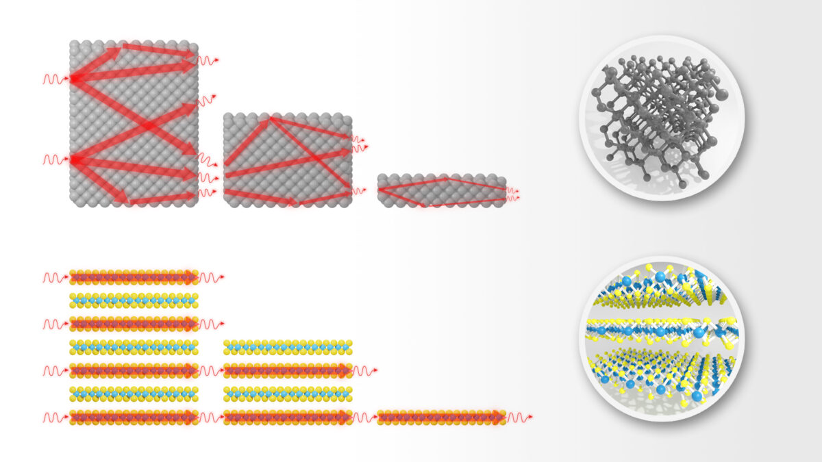
A combined experimental and theoretical study recently published in Advanced Materials investigates the thermal conductivity of molybdenum diselenide (MoSe2), which is an archetypal TMD material. David Saleta Reig, PhD student and first author of the work explains: “We performed a systematic study of the effects of crystal thickness and surrounding environment on heat flow. This fills an important gap in the scientific literature about 2D materials.” Indeed, performing either reliable experimental studies or computer simulations of thermal transport over a broad range of thicknesses from bulk down to a single molecular monolayer is not an easy task. The authors of this research were able to overcome these challenges and produce protocols and results that are valid not only for the case study, MoSe2, but also for a broader range of 2D materials.
Ultrathin MoSe2 transports heat faster than ultrathin silicon
The experimental measurements, in combination with numerical simulations, led to a remarkable result: “We found that the in-plane thermal conductivity of the samples decreases only marginally when reducing the thickness of the crystal all the way to a monolayer with sub-nanometer thickness,” explains Sebin Varghese, PhD student and second author of the study. This behaviour originates from the layered nature of MoSe2 and sets TMD materials apart from non-layered semiconductors, such as the industry standard, silicon. In the latter, the thermal conductivity decreases dramatically when the thickness approaches the nanometer, due to increased scattering at the surface. This effect is much less significant in layered materials, such as MoSe2.
First principles thermal transport simulations reproduced the experimental results in an excellent way, and led to another surprising result: “For the thinnest films, the heat is carried by different phonon modes than for thicker ones,” says Dr Roberta Farris, postdoctoral researcher who developed and carried out the ab initio simulations. Finally, this study also clarifies the influence of the material’s environment on heat dissipation, demonstrating that ultrathin MoSe2 is able to dissipate heat very efficiently to surrounding air molecules.
Dr Klaas-Jan Tielrooij, who coordinated the work, comments: “This work shows that TMD crystals with (sub)nanometer thickness have the potential to outperform silicon films both in terms of electrical and thermal conductivity in this ultrathin limit”. These results thus demonstrate the excellent prospects of TMDs for applications that require thicknesses on the order of a few nanometers or less, for example in the case of flexible and wearable devices and nanoscale electronic components. “Of course it remains to be seen if TMDs will live up to their promises”, concludes Dr Tielrooij, “as there are many hurdles to overcome before these materials will be applied on an industrial scale. At least we now know that their thermal properties are – in principle – not a show-stopper.”
About the study
The authors of this study used the Raman thermometry technique to measure the thermal conductivity of a large set of suspended, crystalline, and clean MoSe2 crystals with systematically varied thickness, taking care to identify and suppress possible thickness-dependent artifacts. They compared the experimental results with ab initio simulations –based on density functional theory and Boltzmann transport theory— performed with the SIESTA method and software, which is particularly suitable for atomistic simulations with a large number of atoms.
This research, coordinated by Dr Klaas-Jan Tielrooij, leader of the ICN2 Ultrafast Dynamics in Nanoscale Systems Group, involved several ICN2 researchers and group leaders belonging to: the Phononic and Photonic Nanostructures Group, led by ICREA Prof. Clivia Sotomayor Torres, the Theory and Simulation Group, led by Prof. Pablo Ordejón, and the Physics and Engineering of Nanodevices Group, led by ICREA Prof. Sergio Valenzuela. Researchers ICFO (Barcelona), Utrecht University (the Netherlands) –with Prof. Zeila Zanolli, former member of Prof. Ordejón’s group—, the University of Liége (Belgium) –with Prof. Matthieu Verstraete, former visiting scientist at ICN2— and the Weizmann Institute of Science (Israel) were also involved.