The award for the best bachelor thesis went to Wiktor Kwapinski (Applied Physics), titled “Improving heat dissipation in hex-SiGe nanowires using 2D hBN flakes.” The jury praised the scientific quality of his work and his new original ideas to solve heat dissipation problems.
Wiktor Kwapiński performed his Bachelor End Project for his studies of Applied Physics at Eindhoven University of Technology in our group during the spring of 2023. He prepared hybrid 1D-2D samples at ICN2 under the direct guidance of Michal Swiniarski, and then performed optical characterization measurements at TU/e under the direct guidance of Marvin van Tilburg.
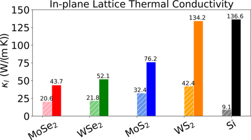
Transition metal dichalcogenides (TMDs) are a class of layered materials that hold great promise for a wide range of applications. Their practical use can be limited by their thermal transport properties, which have proven challenging to determine accurately, both from a theoretical and experimental perspective. We have conducted a thorough theoretical investigation of the thermal conductivity of four common TMDs, MoSe2, WSe2, MoS2, and WS2, at room temperature, to determine the key factors that influence their thermal behavior. We analyze these materials using ab initio calculations performed with the siesta program, anharmonic lattice dynamics and the Boltzmann transport equation formalism, as implemented in the temperature-dependent effective potentials method. Within this framework, we analyze the microscopic parameters influencing the thermal conductivity, such as the phonon dispersion and the phonon lifetimes. The aim is to precisely identify the origin of differences in thermal conductivity among these canonical TMD materials. We compare their in-plane thermal properties in monolayer and bulk form, and we analyze how the thickness and the chemical composition affect the thermal transport behavior. We showcase how bonding and the crystal structure influence the thermal properties by comparing the TMDs with silicon, reporting the cases of bulk silicon and monolayer silicene. We find that the interlayer bond type (covalent vs. van der Waals) involved in the structure is crucial in the heat transport. In two-dimensional silicene, we observe a reduction by a factor ∼15 compared to the Si bulk thermal conductivity due to the smaller group velocities and shorter phonon lifetimes. In the TMDs, where the group velocities and the phonon bands do not vary significantly passing from the bulk to the monolayer limit, we do not see as strong a decrease in the thermal conductivity: only a factor 2–3. Moreover, our analysis reveals that differences in the thermal conductivity arise from variations in atomic species, bond strengths, and phonon lifetimes. These factors are closely interconnected and collectively impact the overall thermal conductivity. We inspect each of them separately and explain how they influence the heat transport. We also study artificial TMDs with modified masses, in order to assess how the chemistry of the compounds modifies the microscopic quantities and thus the thermal conductivity.
Sci. Adv. paper on ultrafast cooling in magic-angle twisted bilayer graphene
Collaborative paper published in Sci. Adv.
A TU/e and Catalan Institute of Nanoscience and Nanotechnology-led collaboration involving researchers from around the world has the answer, and the why, and the results have just been published in the journal Science Advances.
Image: iStockphoto
Electrons carry electrical energy, while vibrational energy is carried by phonons. Understanding how they interact with each other in certain materials, like in a sandwich of two graphene layers, will have implications for future optoelectronic devices. Recent work has revealed that graphene layers twisted relative to each other by a small ‘magic angle’ can act as perfect insulator or superconductor. But the physics of the electron-phonon interactions are a mystery. As part of a worldwide international collaboration, TU/e researcher Klaas-Jan Tielrooij has led a study on electron-phonon interactions in graphene layers. And they have made a startling discovery.
What did the electron say to the phonon between two layers of graphene?
This might sound like the start of a physics meme with a hilarious punchline to follow. But that’s not the case according to Klaas-Jan Tielrooij. He’s an associate professor at the Department of Applied Physics and Science Education at TU/e and the research lead of the new work published in Science Advances.
“We sought to understand how electrons and phonons ‘talk’ to each other within two twisted graphene layers,” says Tielrooij.
Electrons are the well-known charge and energy carriers associated with electricity, while a phonon is linked to the emergence of vibrations between atoms in an atomic crystal.
“Phonons aren’t particles like electrons though, they’re a quasiparticle. Yet, their interaction with electrons in certain materials and how they affect energy loss in electrons has been a mystery for some time,” notes Tielrooij.
But why would it be interesting to learn more about electron-phonon interactions? “These interactions can have a major effect on the electronic and optoelectronic properties of devices, made from materials like graphene, which we are going to see more of in the future.”
Twistronics: Breakthrough of the Year 2018
Tielrooij and his collaborators, who are based around the world in Spain, Germany, Japan, and the US, decided to study electron-phonon interactions in a very particular case – within two layers of graphene where the layers are ever-so-slightly misaligned.
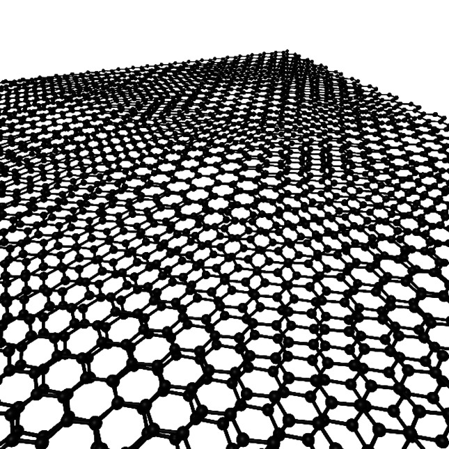
Graphene is a two-dimensional layer of carbon atoms arranged in a honeycomb lattice that has several impressive properties such as high electrical conductivity, high flexibility, and high thermal conductivity, and it is also nearly transparent.
Back in 2018, the Physics World Breakthrough of the Year award went to Pablo Jarillo-Herrero and colleagues at MIT for their pioneering work on twistronics, where adjacent layers of graphene are rotated very slightly relative to each other to change the electronic properties of the graphene.
Twist and astound!
“Depending on how the layers of graphene are rotated and doped with electrons, contrasting outcomes are possible. For certain dopings, the layers act as an insulator, which prevents the movement of electrons. For other doping, the material behaves as a superconductor – a material with zero resistance that allows the dissipation-less movement of electrons,” says Tielrooij.
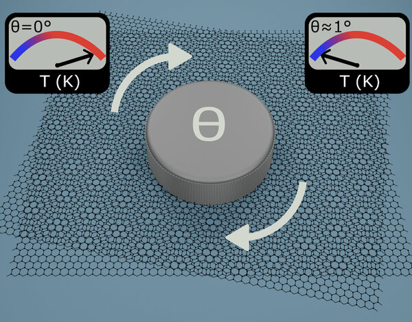
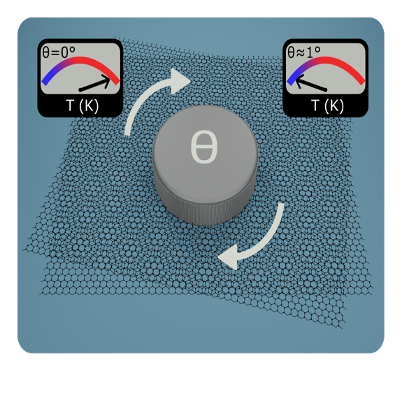
Better known as twisted bilayer graphene, these outcomes occur at the so-called magic angle of misalignment, which is just over one degree of rotation. “The misalignment between the layers is tiny, but the possibility for a superconductor or an insulator is an astounding result.”
Example of graphene layers twisted relative to each other. Image: Klaas-Jan Tielrooij
How electrons lose energy
For their study, Tielrooij and the team wanted to learn more about how electrons lose energy in magic-angle twisted bilayer graphene, or MATBG for short.
To achieve this, they used a material consisting of two sheets of monolayer graphene (each 0.3 nanometers thick), placed on top of each other, and misaligned relative to each other by about one degree.
Then using two optoelectronic measurement techniques, the researchers were able to probe the electron-phonon interactions in detail, and they made some staggering discoveries.
“We observed that the energy vanishes very quickly in the MATBG – it occurs on the picosecond timescale, which is one-millionth of one-millionth of a second!” says Tielrooij.
This observation is much faster than for the case of a single layer of graphene, especially at ultracold temperatures (specifically below -73 degrees Celsius). “At these temperatures, it’s very difficult for electrons to lose energy to phonons, yet it happens in the MATBG.”
We observed that the energy vanishes very quickly in the MATBG – it occurs on the picosecond timescale, which is one-millionth of one-millionth of a second!
Illustration showing the control of energy relaxation with twist angle. Image: Authors
Why electrons lose energy
So, why are the electrons losing the energy so quickly through interaction with the phonons? Well, it turns out the researchers have uncovered a whole new physical process.
“The strong electron-phonon interaction is a completely new physical process and involves so-called electron-phonon Umklapp scattering,” adds Hiroaki Ishizuka from Tokyo Institute of Technology in Japan, who developed the theoretical understanding of this process together with Leonid Levitov from Massachusetts Institute of Technology in the US.
Umklapp scattering between phonons is a process that often affects heat transfer in materials, because it enables relatively large amounts of momentum to be transferred between phonons.
“We see the effects of phonon-phonon Umklapp scattering all the time as it affects the ability for (non-metallic) materials at room temperature to conduct heat. Just think of an insulating material on the handle of a pot for example,” says Ishizuka. “However, electron-phonon Umklapp scattering is rare. Here though we have observed for the first time how electrons and phonons interact via Umklapp scattering to dissipate electron energy.”
The strong electron-phonon interaction is a completely new physical process and involves so-called electron-phonon Umklapp scattering.
Challenges solved together
Tielrooij and collaborators may have completed most of the work while he was based in Spain at the Catalan Institute of Nanoscience and Nanotechnology (ICN2), but as Tielrooij notes. “The international collaboration proved pivotal to making this discovery.”
So, how did all the collaborators contribute to the research? Tielrooij: “First, we needed advanced fabrication techniques to make the MATBG samples. But we also needed a deep theoretical understanding of what’s happening in the samples. Added to that, ultrafast optoelectronic measurement setups were required to measure what’s happening in the samples too.”
The international collaboration proved pivotal to making this discovery.
Tielrooij and the team received the magic-angle twisted samples from Dmitri Efetov’s group at Ludwig-Maximilians-Universität in Munich, who were the first group in Europe able to make such samples and who also performed photomixing measurements, while theoretical work at MIT in the US and at Tokyo Institute of Technology in Japan proved crucial to the success of the research.
At ICN2, Tielrooij and his team members Jake Mehew and Alexander Block used cutting-edge equipment particularly time-resolved photovoltage microscopy to perform their measurements of electron-phonon dynamics in the samples.
The future
So, what does the future look like for these materials then? According to Tielrooij, don’t expect anything too soon.
“As the material is only being studied for a few years, we’re still some way from seeing magic-angle twisted bilayer graphene having an impact on society.”
But there is a great deal to be explored about energy loss in the material.
“Future discoveries could have implications for charge transport dynamics, which could have implications for future ultrafast optoelectronics devices,” says Tielrooij. “In particular, they would be very useful at low temperatures, so that makes the material suitable for space and quantum applications.”
The research from Tielrooij and the international team is a real breakthrough when it comes to how electrons and phonons interact with each other.
But we’ll have to wait a little longer to fully understand the consequences of what the electron said to the phonon in the graphene sandwich.
Review paper on spatiotemporal microscopy published in Adv. Electron. Mater.
Transport phenomena like diffusion, convection, and drift play key roles in the sciences and engineering disciplines. They belong to the most omnipresent and important phenomena in nature that describe the motion of entities such as mass, charge or heat. Understanding and controlling these transport phenomena is crucial for a host of industrial technologies and applications, from cooling nuclear reactors to nanoscale heat-management in the semiconductor industry. For decades, macroscopic transport techniques have been used to access important parameters such as charge mobilities or thermal conductivities. While being powerful, they often require physical contacts, which can lead to unwanted effects. Over the past years, an exciting solution has emerged: a technique called spatiotemporal microscopy (SPTM) that accesses crucial transport phenomena in a contactless, all-optical, fashion. This technique offers powerful advantages in terms of accessible timescales, down to femtoseconds, and length scales, down to nanometres, and, further, selectively observes different species of interest. This tutorial review discusses common experimental configurations of SPTM and explains how they can be implemented by those entering the field. This review highlights the broad applicability of SPTM by presenting several exciting examples of transport phenomena that were unravelled thanks to this technique.
ERC Consolidator Grant of 2 million euros for three TU/e researchers
NOVEMBER 23, 2023
The researchers are all involved in building a digital future that is both fast and energy-efficient
Aida Todri-Sanial, Klaas-Jan Tielrooij en Yoeri van de Burgt. Photos: Vincent van den Hoogen en Angeline Swinkels
TU/e researchers Yoeri van de Burgt, Klaas-Jan Tielrooij, and Aida Todri-Sanial have each been awarded an ERC Consolidator Grant worth two million euros from the European Research Council (ERC). The researchers will use this money for research into organic computers, ultrafast components for wireless networks based on terahertz radiation, and developing a novel computing paradigm based on thermodynamics, respectively. We spoke to the three researchers about their plans for the coming five years.
Associate Professor Yoeri van de Burgt, working at the Department of Mechanical Engineering and institutes EAISI and EHCI, works on electronic systems that are nothing like the electronics in your laptop or cell phone. The heart of the devices in his lab are not made of the semiconductor silicon, but of organic materials that are also found in our bodies.
Moreover, this organic processor is more similar in design to the neural networks in our brains than to a classical computer chip. Van de Burgt now wants to connect such a processor to a biological environment consisting of nerve cells.
That connection to biological material is challenging, according to Van de Burgt. “We want to make a connection that transmits information to both sides, and that’s tricky,” he says. “How do you measure signals from biological cells and pass them on to the processor? Moreover, we want this connection to be ‘self-learning,’ like the flexible connections between brain cells.”
The latter means that the strength of the coupling depends on previous signals that passed through it, but also on the presence of certain neurotransmitters, or signaling substances, in the biological environment.
Yoeri van de Burgt. Photo: Angeline Swinkels
Spikes and neurotransmitters
The platform the researchers are building for this project is several centimeters in size and consists of fluid channels as well as sensors made of so-called mixed conducting polymers that can conduct both electrons and charged ions.
“This processor responds to two types of signals,” Van de Burgt says. “The first type of signals are normal electrical signals – or spikes – from nerve cells. The second signal is neurotransmitters such as dopamine or serotonin, signaling substances that you also find in the brain. The concentration of these substances determines the strength of the learning part.”
Finally, the processor is given a task: the researchers connect a “soft” gripper to it. Not only do they want to control the gripper with electrical signals from the cells. The idea is that the organic processor will eventually “learn” to deal with the gripper and, for example, be able to apply just the right amount of force to grip a particular object.
The promise, according to Van de Burgt, is that in the future the technology could serve for personal prosthetic devices that are directly coupled to the body. This kind of organic computer could eventually do the same work locally, inside the body, much more energy-efficiently than an external classical computer.
The project is called “neuro-labs” and will consist of three PhD students and two postdocs.
Klaas-Jan van Tielrooij. Photo: Vincent van den Hoogen
The power of tetrahertz radiation
Not so long ago people used to only send short text messages to each other; now they talk via video call and send large files effortlessly. This development requires ever faster connections and processing of data. Associate Professor Klaas-Jan Tielrooij of the Department of Applied Physics and Science Education is laying the foundation for wireless electronic components that can keep up with this trend in the future.
New materials and new physics should enable compact transmitters and receivers that process trillions of signals per second. These optoelectronic components use terahertz radiation to send and receive information. In theory, they are many times faster than the components now found in wireless communication networks.
Currently, terahertz components for wireless communications are often inefficient and quite costly. This is in contrast to infrared and optical light, which are widely used in fiber optics. Tielrooij will use extremely thin materials, such as graphene and other so-called quantum materials, which are only one or few atoms thick.
The dynamics of electrons
Essential for a good terahertz transmitter or receiver is an efficient conversion of light of another wavelength to terahertz radiation, and vice versa, and to electrical signals. To this end, Tielrooij is one of the first to apply a design strategy based on the so-called ultrafast thermodynamic properties of materials.
“Existing techniques mostly rely on an interaction between light and the charge of electrons in the material. If you can also use the dynamics of electron temperature then this conversion can be much more efficient,” he says. You can think of this electron temperature as the amount of energy of the electrons.
According to Tielrooij, the components he is developing will soon end up not only in components for wireless networks. Terahertz radiation is also suitable for safely scanning people and suitcases at airports, for example. And it could be used to perform medical scans to detect tumors, for example.
“The terahertz regime is not as developed compared to other wavelengths. It is important that we catch up, because there are many possible applications,” he says.
The project is called “Engineering QUAntum materials for TErahertz applications” (Equate) and consists of three PhD students and two postdocs.
Aida Todri-Sanal. Photo: Vincent van den Hoogen
Self-organizing neural networks
Aida Todri-Sanial, professor of Integrated Circuits in the Department of Electrical Engineering and EAISI, will develop a novel computing paradigm inspired by thermodynamic principles. By applying this to artificial neural networks in the lab this could lead to computers that can solve computationally hard problems in an energy-efficient way.
Todri-Sanial has been modeling and building artificial neural networks in the lab for many years. These are based on electrical oscillators on a chip that uses very little power. Now she wants to give these so-called oscillatory neural networks the ability to learn, similar to how the brain works. This requires rethinking the building blocks of such a system: to enable self-organization, reconfigurability, adaptability, and evolution, something that has not been done before in artificial neural networks.
Efficient and stable
Traits like self-organization, adaptation, and evolution are based on thermodynamics principles, which drive a system to evolve and adapt in an energy-efficient way towards stable configurations. These configurations represent the solution of the task that is given to the system. Self-organization is frequently observed in nature but not yet in our computing systems, Todri-Sanial says.
“In this project, I want to design a computing architecture that self-organizes to solve problems via collective dynamics of coupled oscillators. To do so, we will first develop computing models based on thermodynamics and then design analog integrated circuits for implementing a thermodynamic-inspired computing architecture.”
In the future self-organizing neural networks could solve problems that are typically hard for classical computers, like predicting the weather, find the shortest route between two points on a map or calculating exactly how two molecules will bind. The latter could be very useful in developing new medicines. The research could also lead to more efficient learning strategies for artificial intelligence.
The project “Thermodynamic-inspired computing with oscillatory neural networks” (THERMODON) will consist of three PhD students and three postdocs.
ERC Consolidator Grants
The ERC’s mission is to encourage the highest quality research in Europe through competitive funding and to support frontier research across all fields, based on scientific excellence. ERC grants allow Europe’s brightest minds to identify new opportunities and directions in any field of research and catalyze new and unpredictable scientific and technological discoveries.
The ERC Consolidator Grants are awarded to outstanding researchers of any nationality and age, with at least seven and up to twelve years of experience after a PhD, and a scientific track record showing great promise.
A study led by researchers at the ICN2 and published in ‘ACS Applied Materials & Interfaces’ demonstrates that carbon nanotube networks can be used to provide efficient heat dissipation in applications such as extreme ultraviolet lithography, as well as flexible electronics and interconnects in integrated circuits.
Heat dissipation and low power consumption have become key challenges for modern electronics, which must be addressed hand in hand with the development of new integration and miniaturisation technologies for electronic circuits and systems. In particular, as devices become smaller and more powerful, excess heat issues arise, which can compromise operation and durability. In this context, new materials and nanotechnologies can provide solutions for designing high-performance electronic devices that consume little power and are able to manage heat efficiently.
Carbon nanotube (CNT) networks –an emerging class of nanostructured materials that exhibit outstanding electrical and mechanical properties— are promising candidates for applications requiring efficient heat dissipation, such as extreme ultraviolet (EUV) lithography. EUV lithography is a key technology for the miniaturisation of integrated circuits that requires the use of protective films to avoid damaging photomasks during the process. Suitable materials for these shielding pellicles should be transparent to EUV light, mechanically robust, and thermally stable with high thermal conductivity.
As demonstrated in a research paper published today in ACS Applied Materials & Interfaces, free-standing CNT films are strong candidates for this application, due to their high EUV transparency and ability to withstand heat. The authors of this study –a team of researchers from the ICN2 Ultrafast Dynamics in Nanoscale Systems Group (led by Prof. Klaas-Jan Tielrooij), the former ICN2 Phononic and Photonic Nanostructures Group (led by Prof. Clivia Sotomayor-Torres), and from imec (Leuven, Belgium)— employed all-optical Raman thermometry to gain insight into the thermal properties of free-standing CNT networks.
The authors investigated two types of carbon nanotube films: single-walled CNTs (SWCNTs) and double-walled CNTs (DWCNTs). The first structure consists of a network of nanotubes, whose walls are one atom thick; the second is composed of a network of nanotubes each made of two single-walled nanotubes nested within each other. By Raman thermometry –which is a non-invasive technique— the researchers were able tomeasure the thermal conductivity of these two types of free-standing CNT films at temperatures ranging from 300 K to 700 K.
The study revealed thermal conductivities up to 50 W m−1 K−1 for films made of double-walled CNTs, a remarkable seven times higher than those of single-walled CNT films. “We believe that this enhanced thermal conduction is due to the additional wall in double-walled carbon nanotube networks, which introduces an extra heat-dissipation channel and reduces the impact of defects,” explains Prof. Klaas-Jan Tielrooij, the coordinator of this research and corresponding author of the paper. “Furthermore, the nanotubes in the studied CNT network films were randomly oriented; we think that aligning the double-walled CNTs within the network would lead to even higher thermal conductivity.”
These outcomes show that free-standing carbon nanotube network films, in particular the double-walled one, provide efficient heat dissipation, demonstrating their suitability for application as EUV pellicle materials. In addition, they hold promise for use in flexible electronics and interconnects in integrated circuits. In fact, the relatively high thermal conductivity of these films makes them ideal for efficient thermal management in devices where traditional materials fall short when dimensions are extremely reduced.
Collaborative paper published in Nature Nanotechnology
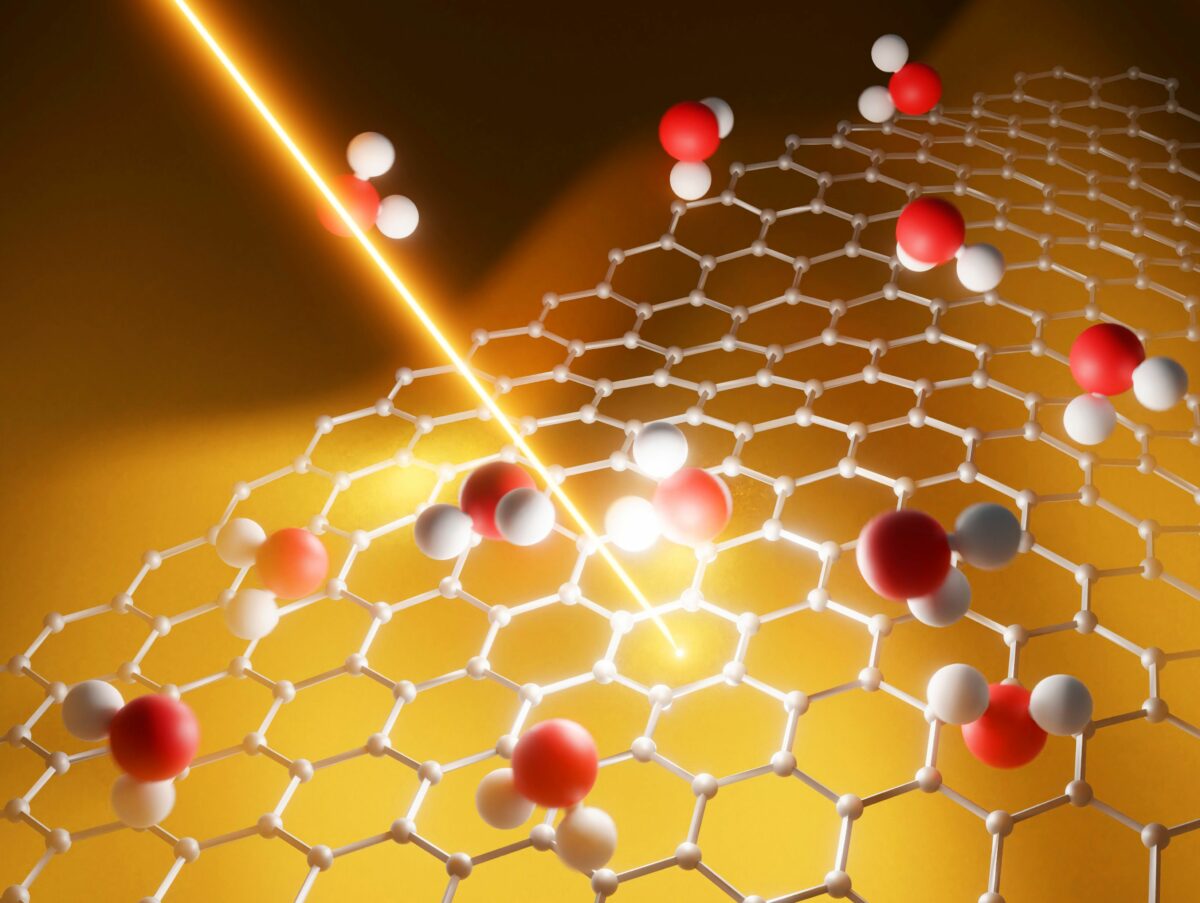
Water and carbon make a quantum couple: the flow of water on a carbon surface is governed by an unusual phenomenon dubbed quantum friction. A work published in ‘Nature Nanotechnology’ experimentally demonstrates this phenomenon –which was predicted in a previous theoretical study— at the interface between liquid water and graphene, a single layer of carbon atoms. These results could lead to applications in water purification and desalination processes and maybe even to liquid-based computers.
For the last 20 years, scientists have been puzzled by how water behaves near carbon surfaces. It may flow much faster than expected from conventional flow theories or form strange arrangements such as square ice. Now, an international team of researchers from the Max Planck Institute for Polymer Research of Mainz (Germany), the Catalan Institute of Nanoscience and Nanotechnology (ICN2, Spain), and the University of Manchester (England), reports in a study published today in Nature Nanotechnology that water can interact directly with the carbon’s electrons: a quantum phenomenon that is very unusual in fluid dynamics.
A liquid, such as water, is made up of small molecules that randomly move and constantly collide with each other. A solid, in contrast, is made of neatly arranged atoms that bathe in a cloud of electrons. The solid and the liquid worlds are assumed to interact only through collisions of the liquid molecules with the solid’s atoms: the liquid molecules do not “see” the solid’s electrons. Nevertheless, just over a year ago, a paradigm-shifting theoretical study proposed that at the water-carbon interface, the liquid’s molecules and the solid’s electrons push and pull on each other, slowing down the liquid flow: this new effect was called quantum friction. However, the theoretical proposal lacked experimental verification.
“We have now used lasers to see quantum friction at work,” explains study lead author Dr Nikita Kavokine, a researcher at the Max Planck Institute in Mainz and the Flatiron Institute in New York. The team studied a sample of graphene – a single monolayer of carbon atoms arranged in a honeycomb pattern. They used ultrashort red laser pulses (with a duration of only a millionth of a billionth of a second) to instantaneously heat up the graphene’s electron cloud. They then monitored its cooling with terahertz laser pulses, which are sensitive to the temperature of the graphene electrons. This technique is called optical pump – terahertz probe (OPTP) spectroscopy.
To their surprise, the electron cloud cooled faster when the graphene was immersed in water, while immersing the graphene in ethanol made no difference to the cooling rate. “This was yet another indication that the water-carbon couple is somehow special, but we still had to understand what exactly was going on,” Kavokine says. A possible explanation was that the hot electrons push and pull on the water molecules to release some of their heat: in other words, they cool through quantum friction. The researchers delved into the theory, and indeed: water-graphene quantum friction could explain the experimental data.
“It’s fascinating to see that the carrier dynamics of graphene keep surprising us with unexpected mechanisms, this time involving solid-liquid interactions with molecules none other than the omnipresent water,” comments Prof Klaas-Jan Tielrooij from ICN2 (Spain) and TU Eindhoven (The Netherlands). What makes water special here is that its vibrations, called hydrons, are in sync with the vibrations of the graphene electrons, called plasmons, so that the graphene-water heat transfer is enhanced through an effect known as resonance.
The experiments thus confirm the basic mechanism of solid-liquid quantum friction. This will have implications for filtration and desalination processes, in which quantum friction could be used to tune the permeation properties of the nanoporous membranes. “Our findingsare notonly interesting for physicists, but they also hold potential implications for electrocatalysis and photocatalysis at thesolid-liquid interface,” says Xiaoqing Yu, PhD student at the Max Planck Institute in Mainz and first author of the work.
The discovery was down to bringing together an experimental system, a measurement tool and a theoretical framework that seldom go hand in hand. The key challenge is now to gain control over the water-electron interaction. “Our dream is to switch quantum friction on and off on demand,” Kavokine says. “This way, we could design smarter water filtration processes, or perhaps even fluid-based computers.”
A study carried out by researchers from the HZDR Institute of Radiation Physics, ICN2 Ultrafast Dynamics in Nanoscale Systems group, University of Exeter Centre for Graphene Science, and TU Eindhoven demonstrates that graphene-based materials can be used to efficiently convert high-frequency signals (in the terahertz regime) into visible light, and that this mechanism is tunable. These outcomes open the path to exciting applications in next-future information and communication technologies.
The ability to convert signals from one frequency regime to another is key to various technologies, in particular in telecommunications, where, for example, data processed by electronic devices are often transmitted as optical signals through fibres. To enable significantly higher data transmission rates, future 6G wireless communication systems will need to extend the carrier frequency above 100GHz up to the terahertz (THz) range. Therefore, a fast and controllable mechanism to convert THz waves into visible or telecom light will be required. Imaging and sensing technologies could also benefit from it.
What is missing is a material that is capable of upconverting photon energies by a factor of 1000 or so: from the milli-electronvolt (meV) range to around 1 eV. Researchers have recently identified the strong nonlinear response of so-called Dirac quantum materials, e.g. graphene and topological insulators, to THz light pulses (see this and this previous news item). This manifests in the highly efficient generation of high harmonics upon excitation with THz pulses. These harmonics are still within the THz range, however, there were also first observations of visible light emission from graphene upon infrared and terahertz excitation. Up to now, this effect was extremely inefficient and the underlying physical mechanism was not understood.
A work published in Nano Letters demonstrates ultrafast and tunable conversion of THz light into visible light in graphene systems. The study was led by Dr Igor Ilyakov and Dr Sergey Kovalev–from the Helmholtz-Zentrum Dresden-Rossendorf (HZDR, Germany)— and by Prof Klaas-Jan Tielrooij –group leader at Catalan Institute of Nanoscience and Nanotechnology (ICN2, Spain) and Eindhoven University of Technology (The Netherlands). They provide a physical explanation for this mechanism and show how the light emission can be strongly enhanced by using highly doped graphene (so-called GraphExeter) and by using a grating-graphene metamaterial. They also observed that the conversion occurs very rapidly –on the sub-nanosecond time scale— and that it can be controlled by electrostatic gating.
The authors ascribe the light frequency conversion in graphene to a THz-induced thermal radiation mechanism: the charge carriers absorb electromagnetic energy from the incident THz field; the absorbed energy rapidly distributes in the material, resulting in carrier heating; finally, this leads to emission of photons in the visible spectrum as a result of black-body radiation.
The tunability and speed of the THz-to-visible light conversion achieved in graphene-based materials has great potential for application in information and communication technologies. The underlying ultrafast thermodynamic mechanism could certainly produce an impact on THz-to-telecom interconnects, as well as in any technology that requires ultrafast frequency conversion of signals.
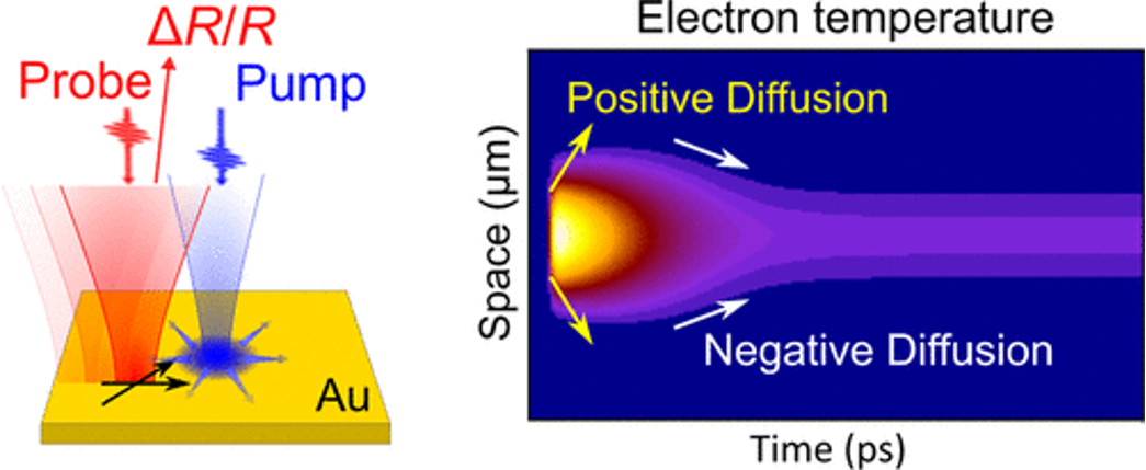
Ultrafast light-induced spatiotemporal dynamics in metals in the form of electron and/or phonon heating is a fundamental physical process that has tremendous practical relevance. In particular, understanding the resulting lateral heat transport is of key importance for various (opto)electronic applications and thermal management but has attracted little attention. Here, by using scanning ultrafast thermo-modulation microscopy to track the spatiotemporal electron diffusion in thin gold films, we show that a few picoseconds after the optical pump there is unexpected heat flow from phonons to electrons, accompanied by negative effective thermal diffusion, characterized by shrinking of the spatial region with increased temperature. Peculiarly, this occurs on the intermediate time scale, between the few picosecond long thermalization stage and the many picosecond stage dominated by thermoacoustic vibrations. We accurately reproduced these experimental results by calculating the spatiotemporal photothermal response based on the two-temperature model and an improvement of the standard permittivity model for gold. Our findings facilitate the design of nanoscale thermal management strategies in photonic, optoelectronic, and high-frequency electronic devices.

![[Translate to English:]](https://assets.w3.tue.nl/w/fileadmin/_processed_/7/0/csm_Tielrooij%20Banner%20image%20Graphene%20iStockphoto_205c0279f2.jpg "[Translate to English:]")