Ultra-efficient heat dissipation thanks to graphene electrons

Collaborative ICFO-ICN2-BIST paper published in Nature Nanotechnology.

The continuous miniaturization and integration of electronic circuits in mobile phones, computers etc. leads to increasingly strong demands for thermal management: Dissipating excess heat is required to guarantee the correct functioning of the devices. Research published today in Nature Nanotechnology reveals that graphene enables ultra-efficient heat dissipation, spreading heat over micrometers during a time as short as a few hundred femtoseconds – less than a millionth of a millionth of a second. This could make it possible to efficiently cool down local circuit elements, such as transistors, of (opto)electronic devices.

Graphene is known to possess one of the highest thermal conductivities: a few thousand W/m2K – even higher than diamond. This is due to heat transported by lattice vibrations, while the contribution of charge carriers – electrons and holes – is typically small. However, graphene had something up its sleeve: an unconventional transport regime called the hydrodynamic regimewhere an even higher thermal conductivity, with heat carried by charges, is possible. In this hydrodynamic regime, charges interact strongly with each other, and follow similar laws as those that apply to classical fluid transport. 

Within this regime – under certain conditions – the quantum-critical Dirac fluid regime exists, where the system no longer behaves similarly to a classical fluid. What is special about this regime is that if the electronic system is heated up, hot electrons and hot holes coexist and move in the same direction under a thermal gradient, conserving total momentum. This enables heat spreading that is much more efficient than in other transport regimes. Until now, attempts to observe this at room temperature had not been successful

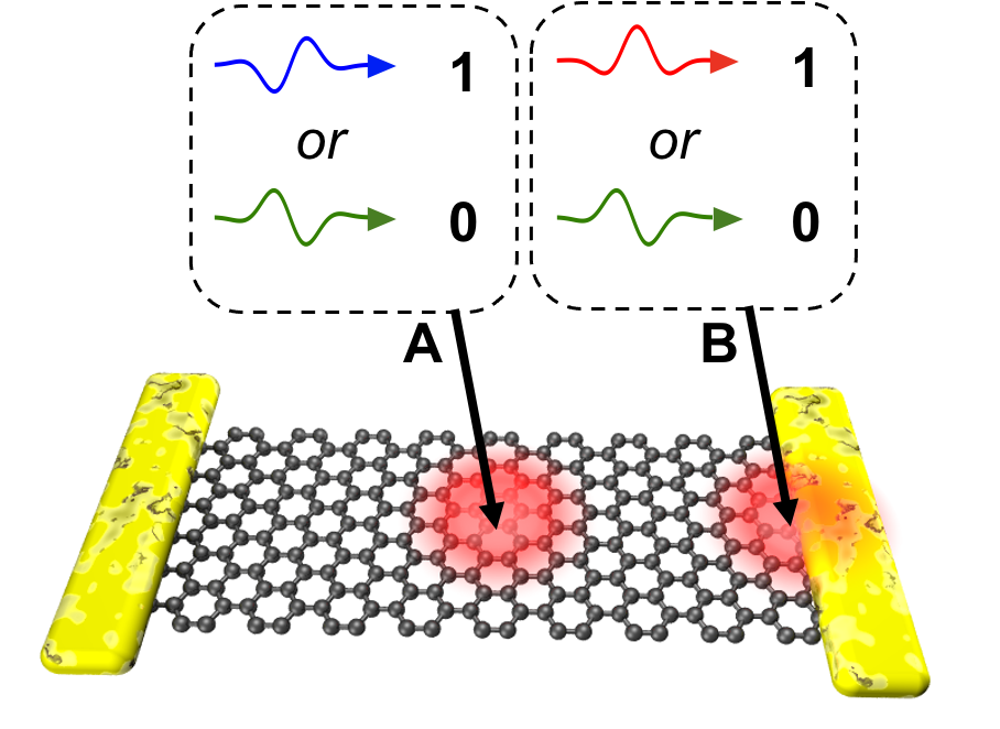
The authors of this work were able to follow heat transport in graphene (specifically, in a graphene device encapsulated by hexagonal boron nitride) at room temperature by means of a technique called ultrafast spatiotemporal thermoelectric microscopy. “The breakthrough that enabled us to observe electronic heat spreading in graphene at room temperature was using ultrashort light pulses, offset in space and time with nanometer and femtosecond accuracy, respectively, while measuring the generated thermoelectric current”, explains Dr Alexander Block. The researchers first demonstrated that their technique gave the expected heat spreading when examined in the common diffusive regime. Then they studied the hydrodynamic regime, where they observed strongly enhanced heat spreading, corresponding to a giant thermal diffusivity and an electronic thermal conductivity exceeding the record-high lattice thermal conductivity.  

The scientists moreover demonstrated the ability to control the amount of heat spreading by tuning the system in and out of the Dirac fluid regime. For this, they varied independently the laser power –which translates to a modification of the electron temperature –  and the voltages applied to the device through electrical gates – which act on another important graphene parameter, called the Fermi energyThis controllable transition between different heat spreading regimes at room temperature and the giant thermal diffusivity had not been observed before. “It is amazing to see that hydrodynamic phenomena that until a few years ago were experimentally inaccessible, are now reachable at room temperature, using standard encapsulated graphene, and even potentially useful for real-life applications in thermal management,” concludes Dr Klaas-Jan Tielrooij, coordinator of the work and Junior Group Leader at ICN2. These applications in thermal management would exploit the ultra-efficient heat spreading observed in graphene to extract heat from local hot spots in (opto)electronic circuitry in a broad range of devices used for information and communications technology. 

This research is the result of a collaboration between the Institute of Photonic Sciences (ICFO) and the Catalan Institute of Nanoscience and Nanotechnology (ICN2), both part of the Barcelona Institute of Science and Technology in Spain. The work was  coordinated by Dr Klaas-Jan Tielrooij, group leader at ICN2, in collaboration with ICREA Profs. Niek van Hulst and Frank Koppens at ICFOand Stephan Roche at ICN2. The first author of the paper is Dr Alexander Block who is affiliated to both ICFO and ICN2. This work also involved Alessandro Principi from the University of Manchester (UK) and researchers from the National Institute for Materials Science of Tsukuba (Japan).

Congratulations to Xiaoyu!

PhD defended at UvA (NL)

Dr. Xiaoyu Jia has just successfully defended his PhD at the University of Amsterdam (NL). His project was a collaboration between ICN2 and the Max Planck Institute of Polymer Research (MPIP) in Mainz (DE), supervised by Mischa Bonn and Hai I. Wang at the MPIP and Klaas-Jan Tielrooij at ICN2. Congrats!

New insights into charge carrier dynamics in graphene-based materials for optoelectronic applications

Collaborative paper published in ACS Nano.

A study published in “ACSNano” investigates the mechanism governing the cooling dynamics of photo-excited charge carriers in graphene-based structures, which are interesting candidates for future optoelectronic devices. This research was led by Dr Klaas-Jan Tielrooij, leader of the ICN2 Ultrafast Dynamics in Nanoscale Systems Group.

Various emerging technologies for optoelectronic applications, in particular in the field of data communication, take advantage of the ultrafast dynamics of photo-excited charge carriers in graphene. After reaching an excited state by photon absorption, these carriers undergo a multi-step relaxation phase, in which they release the extra energy they acquired and return to their ground state. First, scattering between carriers occurs, which leads to a state with an elevated electronic temperature. Then, these hot charge carriers cool down to room temperature via various processes. Large research efforts have been devoted to the identification of the physical mechanisms that drive this cooling phase, which depends on how graphene is prepared and by the materials that surround it. The cooling processes include interactions with graphene optical and acoustic phonons, and with substrate phonons in nearby materials. A deep understanding of the phenomena governing this phase is key to graphene’s use in optoelectronic devices.

In a paper recently published in ACSNano, the cooling dynamics of hot carriers are studied in two technologically relevant material systems based on high-quality graphene. This work, carried out by an international team of researchers from various institutes in Spain, Italy, Germany, UK, Belgium and China, and coordinated by Dr Klaas-Jan Tielrooij, leader of the ICN2 Ultrafast Dynamics in Nanoscale Systems Group, revealed the crucial role played by a cooling process in particular, which is always present in graphene, thus providing the intrinsic limit of the lifetime of its electronic excitations.

Using three different time-resolved optical measurement techniques, the researchers analysed the behaviour of photo-induced hot carriers in WSe2-encapsulated graphene, where graphene is sandwiched between two layers of tungsten diselenide, and in suspended graphene, grown by chemical vapour deposition. Both systems are meant for applications requiring very high quality of graphene, which implies large charge mobility. In these materials, a cooling timescale of tens of picoseconds was expected, because the so-called “disorder-assisted supercollision cooling” is relatively inefficient in high-mobility graphene, and because, in the two cases under study, graphene interacts weakly with phonons in its environment. The experimental results, though, showed that in both samples the relaxation of hot carriers occurs in a few (2-4) picoseconds, a much shorter time than expected.

To explain these outcomes, the authors of the study suggest that another cooling mechanism intrinsic to graphene, involving optical phonon emission, is at work. Specifically, hot carriers initially decay by emitting optical phonons, and, in turn, these optical phonons couple to acoustic phonons, producing a slower decay.  In the meanwhile, the electronic system undergoes a continuous rethermalization (a process that leads to thermal equilibrium). This enable constant emission of optical phonons, which therefore provides a continuous heat sink. The researchers also developed an analytical modelof this cooling pathway, which fits well with the experimental results and indicates what are the key parameters to play with for slowing down or accelerating the charge carriers relaxation.

This study provides fundamental insights into the hot-carrier cooling dynamics in high-quality graphene, which will be extremely useful for the future development of graphene-based optoelectronic devices.

Not all 2D materials are as strong as graphene: Transition Metal Dichalcogenides get weaker when thickness decreases

Paper published in Adv. Mater.

A new study recently published in “Advanced Materials” reveals that MoSe2, a prominent material of the transition metal dichalcogenides (TMDs) family, loses relative stiffness when its thickness is reduced. This work was carried out by researchers from the Adam Mickiewicz University (AMU) in Poznan (Poland) and the ICN2, under the coordination of Dr Bartlomiej Graczykowski and Dr Klaas-Jan Tielrooij, respectively.

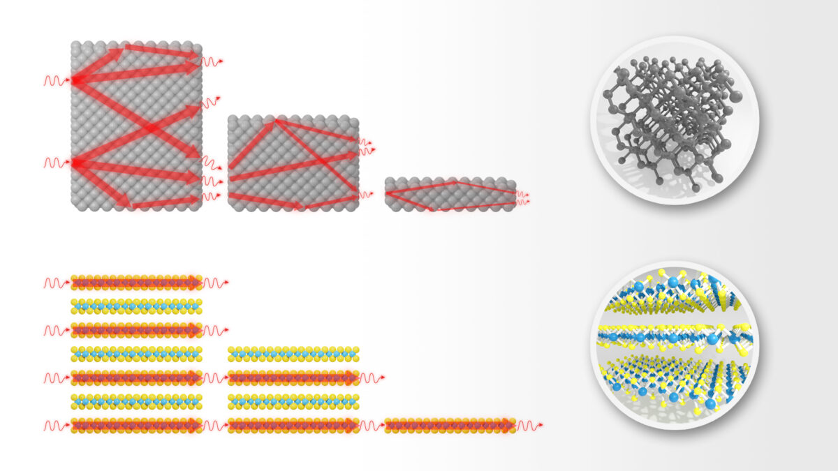
Since the discovery of graphene, a wonder material exhibiting remarkable properties due to its being as thin as a single layer of atoms, a wide variety of new 2D materials have been fabricated and studied. The general expectation is that, as for graphene, such materials’ mechanical properties are superior to their bulk counterparts. However, this is not the case for molybdenum diselenide (MoSe2), one of the most attractive members of the transition metal dichalcogenides (TMD) family, which on the contrary becomes increasingly softer when made thinner.

These results, which contradict the common assumption that relative mechanical strength increases at the nanoscale, were reported in a paper recently published in the journal Advanced Materials. The study was coordinated by Dr Bartlomiej Graczykowski, from the Adam Mickiewicz University (AMU) in Poznan (Poland), and Dr Klaas-Jan Tielrooij, leader of the ICN2 Ultrafast Dynamics in Nanoscale Systems group. “Our findings are extraordinary since they clearly show a progressive softening of MoSe2 while reducing its thickness from bulk to three molecular layers,” explains Visnja Babacic, Ph.D. student at AMU and first author of the paper.

The research team was able to study the elastic properties of various samples of MoSe2, of progressively thinner dimensions, by means of a technique called micro-Brillouin light scattering. This contactless and non-destructive analysis method uses the interaction of light with vibrations in the material (acoustic waves in the gigahertz regime) to extract information about its mechanical characteristics. “It is a more reliable and perhaps more useful technique than traditional contact methods,” comments Dr Bartolomej Graczykowski, leader of the project at AMU, “since it can provide both mechanical information and thickness values of the membranes.” The same approach could also be used to study other van der Waals (vdW) materials.

This elastic softening of the material when decreasing the thickness of the sample, called the elastic size effect, has profound implications for the design and development of nanodevices –such as nanomechanical resonators for sensors–, where mechanical properties are essential for their durability and robust performance. “The results of our study are also highly relevant for related research fields, such as nanoscale thermal transport, electronics, or resonators employing vdW materials,” highlights Dr Klaas-Jan Tielrooij, leader of the project at the ICN2.

Enhanced Perovskite Solar Cells: new insights into defects’ impact on stability

Collaborative paper published in Joule.

Title: Decoupling the effects of defects on efficiency and stability through phosphonates in stable halide perovskite solar cells

Abstract:

Understanding defects is of paramount importance for the development of stable halide perovskite solar cells (PSCs). However, isolating their distinctive effects on device efficiency and stability is currently a challenge. We report that adding the organic molecule 3-phosphonopropionic acid (H3pp) to the halide perovskite results in unchanged overall optoelectronic performance while having a tremendous effect on device stability. We obtained PSCs with ∼21% efficiency that retain ∼100% of the initial efficiency after 1,000 h at the maximum power point under simulated AM1.5G illumination. The strong interaction between the perovskite and the H3pp molecule through two types of hydrogen bonds (HI and OH) leads to shallow point defect passivation that has a significant effect on device stability but not on the non-radiative recombination and device efficiency. We expect that our work will have important implications for the current understanding and advancement of operational PSCs.

Featured among “Nanoscale Emerging Investigators 2021”

Review article on Hot Carriers in Graphene published in Nanoscale collection by promising early-career researchers.

Nanoscale Emerging Investigators 2021 collection with invited contribution from ICN2 Junior Group Leader Klaas-Jan Tielrooij

The journal Nanoscale is currently presenting its themed issue Emerging Investigators 2021 “highlighting 2021’s rising stars of nanoscience and nanotechnology research. This issue gathers the very best work from researchers in the early stages of their independent career. Each contributor was recommended by experts in their fields for carrying out work with the potential to influence future directions in nanoscience and nanotechnology.”

One of the articles in the themed collection is a contribution from ICN2 Junior Group Leader Klaas-Jan Tielrooij, with a review article on “Hot Carriers in Graphene – Fundamentals and Applications”. The review is written together with three colleagues from Canada, the UK, and Germany. Hot carriers in graphene exhibit fascinating physical phenomena and offer great promise for exciting optoelectronic and photonic applications. In particular, hot-carrier-enabled processes that give rise to the emission, conversion, and detection of light can have a disruptive impact, for example in the field of data communication, high-frequency electronics, and industrial quality control. The review describes the current status of the field, and is aimed at a broad audience, including prospective students as well as scientists, engineers and technologists from both academia and industry. 

News & Views: Hot plasmons make graphene shine

News & Views piece published in Nature Materials

A new significant research on ultrafast excitation and relaxation mechanisms in graphene, published in the current issue of “Nature Materials”, is featured in the “News & Views” section of the journal in an introductive article by ICN2 group leader Dr Klaas-Jan Tielrooij and ICFO group leader Prof. Frank Koppens.

Dr Klaas-Jan Tielrooij, leader of the ICN2 Ultrafast Dynamics in Nanoscale Systems group, and Prof. Frank Koppens, group leader at the Institute of Photonic Sciences (ICFO), published a News & Views article in Nature Materials as an introduction to highlight a paper published in the same issue of the journal.  The work they summarize is a remarkable study on the ultrafast carrier dynamics of graphene, carried out by Dr Laura Kim –from the Massachusetts Institute of Technology– and her colleagues, which provides the first experimental evidence of hot plasmon emission in graphene as a consequence of carrier excitation by ultrashort laser pulses.  

When graphene carriers are excited, carrier-carrier interactions take place on a femtosecond timescale. A cooling phase follows, which can occur through different processes, chiefly via phonon emission. According to this research, an additional relaxation (and cooling) channel exists, which involves ultrafast energy flow from excited carriers into graphene plasmons. This process leads to the emission of mid-infrared light, which increases its brightness when gold nanodisks are added.

As highlighted by Dr Tielrooij and Prof. Koppens, this study is not only noteworthy in its own rights, but also for the opportunities of new practical applications that the identified mechanism provides.

Image credit: Matteo Ceccanti

Electrical tunability of terahertz nonlinearity in graphene

Collaborative paper published in Science Advances.

Abstract:

Graphene is conceivably the most nonlinear optoelectronic material we know. Its nonlinear optical coefficients in the terahertz frequency range surpass those of other materials by many orders of magnitude. Here, we show that the terahertz nonlinearity of graphene, both for ultrashort single-cycle and quasi-monochromatic multicycle input terahertz signals, can be efficiently controlled using electrical gating, with gating voltages as low as a few volts. For example, optimal electrical gating enhances the power conversion efficiency in terahertz third-harmonic generation in graphene by about two orders of magnitude. Our experimental results are in quantitative agreement with a physical model of the graphene nonlinearity, describing the time-dependent thermodynamic balance maintained within the electronic population of graphene during interaction with ultrafast electric fields. Our results can serve as a basis for straightforward and accurate design of devices and applications for efficient electronic signal processing in graphene at ultrahigh frequencies

Defects to the rescue in graphene/WS2 heterostructures

Collaborative paper published in Science Advances.

Title: Long-lived charge separation following pump-wavelength-dependent ultrafast charge transfer in graphene/WS2 heterostructures

Abstract:

Van der Waals heterostructures consisting of graphene and transition metal dichalcogenides have shown great promise for optoelectronic applications. However, an in-depth understanding of the critical processes for device operation, namely, interfacial charge transfer (CT) and recombination, has so far remained elusive. Here, we investigate these processes in graphene-WS2 heterostructures by complementarily probing the ultrafast terahertz photoconductivity in graphene and the transient absorption dynamics in WSfollowing photoexcitation. We observe that separated charges in the heterostructure following CT live extremely long: beyond 1 ns, in contrast to ~1 ps charge separation reported in previous studies. This leads to efficient photogating of graphene. Furthermore, for the CT process across graphene-WSinterfaces, we find that it occurs via photo-thermionic emission for sub-A-exciton excitations and direct hole transfer from WSto the valence band of graphene for above-A-exciton excitations. These findings provide insights to further optimize the performance of optoelectronic devices, in particular photodetection.

Grating-graphene metamaterial for THz nonlinear photonics

Collaborative paper published in ACS Nano.

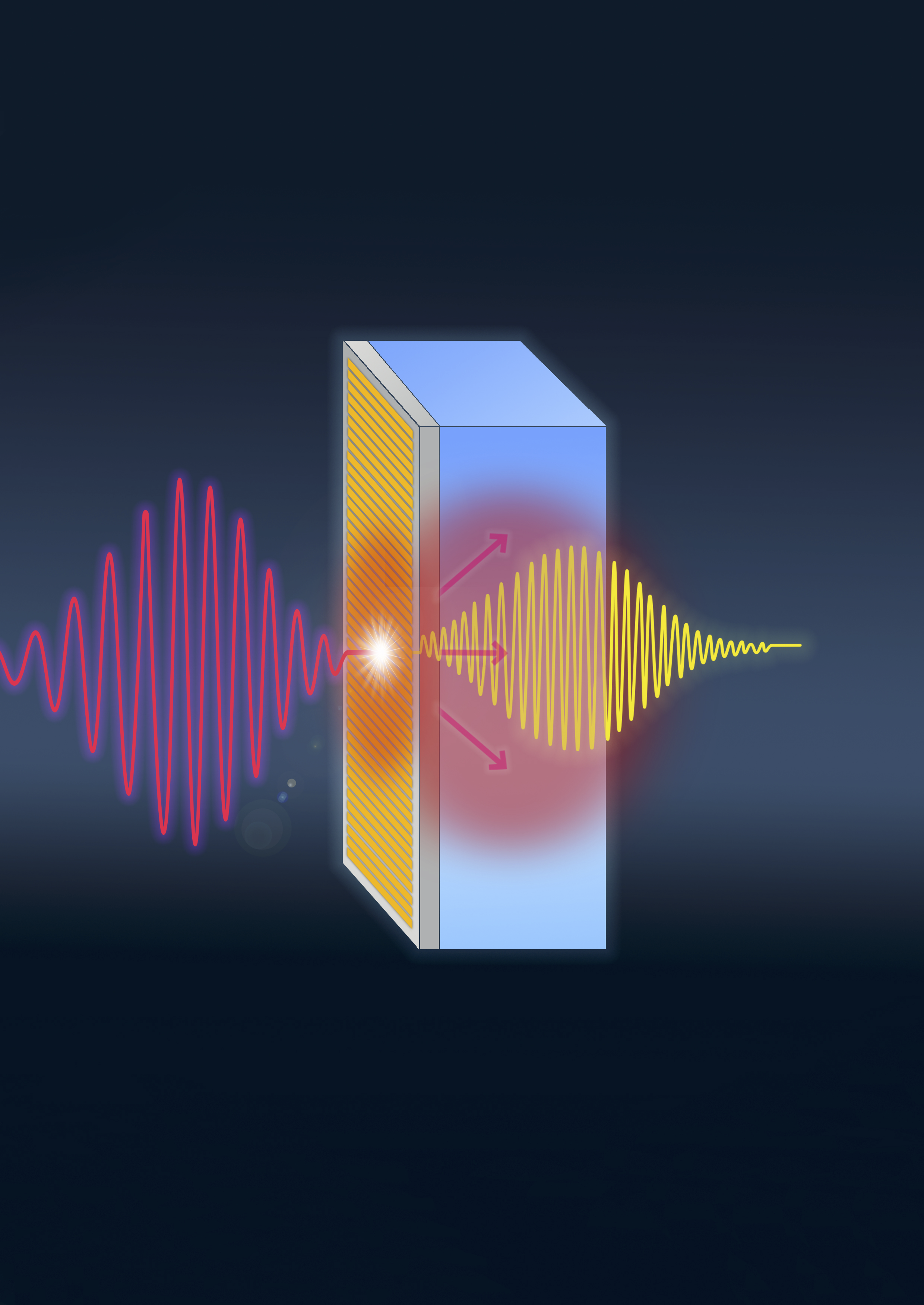
Researchers from various institutes in Barcelona and Germany have demonstrated that a hybrid material consisting of a monolayer of graphene and a metallic grating structure is an excellent candidate for relevant commercial applications in which efficient nonlinear conversion of (invisible) terahertz light is required. This work has just been published in ACSNano, in a paper with Dr Klaas-Jan Tielrooij, leader of the ICN2 Ultrafast Dynamics in Nanoscale Systems group, as last author. A metal grating combined with graphene opens up the road to terahertz nonlinear photonic applications. 

Nonlinear optical conversion – i.e. the process by which an incident light beam of a certain wavelength turns into rays of different wavelengths, due to its interaction with the material it passes through – is relevant to for many current and future technologies, such as imaging, information storage and processing, telecommunication, quantum technologies, and other fields.

The ideal material for these applications should provide, first of all, a very high conversion efficiency, which means that a significant fraction of the incoming beam has to be converted into light of the desired wavelengths. It is also required to have a small footprint (that is, as little material as possible has to be used); to be compatible with standard CMOS technology used in most electronic devices; and to be able to operate at room temperature. Particularly needed is an optimal solution for applications in which the incident light is in the terahertz (THz) region of the electromagnetic spectrum. This light cannot be seen by the human eye, yet it is commonly used for applications ranging from airport security to product inspection, and can play an important role in future communication technologies.

Two-dimensional materials are highly interesting for light conversion. They consist of a single layer (or a couple of them) of atoms and thus have almost zero-thickness (this is why they are called 2D materials). This characteristic ensures a small material footprint. In addition, since they are thinner than the wavelength of light, the optical waves propagating in these materials remain in phase. Among them, graphene, a by-now-well-known material made of a monolayer of carbon atoms arranged in a honeycomb structure, is particularly promising. This is because it exhibits very large nonlinear conversion coefficients, especially in the THz range. On the other hand, though, its extremely reduced thickness affects its conversion efficiency, due to the small quantity of matter the light can interact with. To overcome this problem, the authors decided to combine graphene with another material system that enhances this interaction.

A team of researchers from the Catalan Institute of Nanoscience and Nanotechnology (ICN2, Spain), the Helmholtz-Zentrum Dresden-Rossendorf  (HZDR, Germany), the Institute of Photonic Sciences (ICFO, Spain), the Max Planck Institute of Polymer Research, Mainz (Germany), the University of Bielefeld (Germany) and the Technical University of Berlin (TUB, Germany) have combined graphene with a metallic structure that provides field-enhancement, leading to a hybrid material characterized by very high nonlinear light conversion efficiency. As explained in a scientific article recently published in ACSNano, this structure (grating-graphene) produces outcoming light at the new wavelength having an intensity more than 1000 times higher than the one obtained using just graphene.

Dr Klaas-Jan Tielrooij, leader of the ICN2 Ultrafast Dynamics in Nanoscale Systems group and last author of the paper explains: “The combination of graphene and a metal grating leads to highly efficient conversion of terahertz light, reaching up to 1% (in field) for rather weak incident light.” Dr Jan-Christoph Deinert, from HZDR, first author of the work, adds: “This hybrid material made it possible for us to observe light that oscillates three times, five times, seven times, and even nine times faster than the incoming light.

The outstanding conversion efficiency of this hybrid material guarantees low power consumption in the conversion process, while the compatibility of graphene with CMOS technology allows for integration in devices based on such technology. Overall, this grating-graphene structure presents itself as an excellent candidate for commercially viable applications requiring nonlinear conversion in the terahertz regime, chip-integration, room temperature operation and low power consumption.

Image credit and copyright: HZDR / Werkstatt X