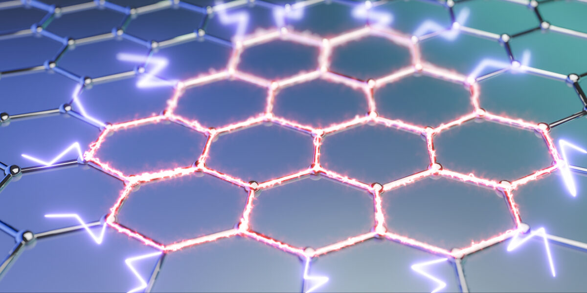
Plasmonic antenna coupling to hyperbolic phonon-polaritons for sensitive and fast mid-infrared photodetection with graphene

Collaborative paper published in Nature Communications.

Abstract:

Integrating and manipulating the nano-optoelectronic properties of Van der Waals heterostructures can enable unprecedented platforms for photodetection and sensing. The main challenge of infrared photodetectors is to funnel the light into a small nanoscale active area and efficiently convert it into an electrical signal. Here, we overcome all of those challenges in one device, by efficient coupling of a plasmonic antenna to hyperbolic phonon-polaritons in hexagonal-BN to highly concentrate mid-infrared light into a graphene pn-junction. We balance the interplay of the absorption, electrical and thermal conductivity of graphene via the device geometry. This approach yields remarkable device performance featuring room temperature high sensitivity (NEP of 82 pW/√Hz) and fast rise time of 17 nanoseconds (setup-limited), among others, hence achieving a combination currently not present in the state-of-the-art graphene and commercial mid-infrared detectors. We also develop a multiphysics model that shows very good quantitative agreement with our experimental results and reveals the different contributions to our photoresponse, thus paving the way for further improvement of these types of photodetectors even beyond mid-infrared range.

Fast electrical modulation of erbium emitter decay rates using graphene

Collaborative paper published in Nature Communications.

Crystals doped with rare-earth ions, such as erbium (Er3+), play an important role for existing and future technologies. For example, erbium-doped fibers are crucial for optical communications systems carrying information as optical signals over long distances. Rare-earth ions furthermore have several properties that make them highly promising and quantum technologies, such as long lifetimes and long decoherence times. Indeed, systems based on rare-earth ions are gaining increasing attention for serving, for example, as quantum bits and quantum memories. 

Scientists at ICFO (Spain), CNRS (France) and ICN2 (Spain) have now made several breakthroughs regarding novel quantum and plasmonic applications based on nanoscale rare-earth-ion systems. In particular, they have managed to create erbium emitter layers of nanoscale thickness (~10 nm) with emission properties that are similar to those of bulk emitter materials. Owing to the very small layer thickness, the emitters can efficiently interact with their environment. By exploiting this property, the researchers have created nanophotonic devices where the environment of the nanolayer of emitters is formed by electrically tunable monolayer graphene. These hybrid erbium-graphene devices allow for extremely strong emitter-environment interactions via dipole-dipole coupling. This interaction is so strong that for a large fraction of the erbium emitters the decay is enhanced by a factor of more than 1000. This means that more than 99.9% of the energy flows from excited emitters to graphene. 

Besides providing a platform for very strong emitter-environment interactions, the hybrid devices allow for tuning the Fermi energy of graphene in a dynamical fashion using a small electrical voltage. As a result, the interaction strength can be controlled with a high modulation frequency – up to 300 kHz. Remarkably, this is more than three orders of magnitude faster than the natural decay rate of excited erbium ions. Furthermore, the energy flow pathway can be controlled with this high modulation frequency, where excited ions lead to mainly electron-hole pair creation or to plasmon launching in graphene. Thus, the device allows for temporal control of plasmon launching, as well as creating controlled waveforms, with applications in plasmonic and quantum technologies. 

The results have been recently published in Nature Communications under the study “Fast electrical modulation of strong near-field interactions between erbium emitters and graphene.” The work was carried out within the framework of the Horizon2020 FET Open project “NanOQTech” (2016-2019) that aimed to establish nanoscale rare-earth systems as a novel material platform for various technological applications. 

Kinetic Ionic Permeation and Interfacial Doping of Supported Graphene

Collaborative paper published in Nano Letters.

Abstract:

Due to its outstanding electrical properties and chemical stability, graphene finds widespread use in various electrochemical applications. Although the presence of electrolytes strongly affects its electrical conductivity, the underlying mechanism has remained elusive. Here, we employ terahertz spectroscopy as a contact-free means to investigate the impact of ubiquitous cations (Li+, Na+, K+, and Ca2+) in aqueous solution on the electronic properties of SiO2-supported graphene. We find that, without applying any external potential, cations can shift the Fermi energy of initially hole-doped graphene by ∼200 meV up to the Dirac point, thus counteracting the initial substrate-induced hole doping. Remarkably, the cation concentration and cation hydration complex size determine the kinetics and magnitude of this shift in the Fermi level. Combined with theoretical calculations, we show that the ion-induced Fermi level shift of graphene involves cationic permeation through graphene. The interfacial cations located between graphene and SiO2 electrostatically counteract the substrate-induced hole doping effect in graphene. These insights are crucial for graphene device processing and further developing graphene as an ion-sensing material.

THz nonlinear optics of graphene

Collaborative paper published in Advanced Optical Materials.

Abstract:

Graphene has long been predicted to show exceptional nonlinear optical properties, especially in the technologically important terahertz (THz) frequency range. Recent experiments have shown that this atomically thin material indeed exhibits possibly the largest nonlinear coefficients of any material known to date, paving the way for practical graphene-based applications in ultrafast (opto-)electronics operating at THz rates. Here the advances in the booming field of nonlinear THz optics of graphene are reported, and the state-of-the-art understanding of the nature of the nonlinear interaction of graphene with the THz fields based on the thermodynamic model of electron transport in graphene is described. A comparison between different mechanisms of nonlinear interaction of graphene with light fields in THz, infrared, and visible frequency ranges is also provided. Finally, the perspectives for the expected technological applications of graphene based on its extraordinary THz nonlinear properties are summarized. This report covers the evolution of the field of THz nonlinear optics of graphene from the very pioneering to the state-of-the-art works. It also serves as a concise overview of the current understanding of THz nonlinear optics of graphene and as a compact reference for researchers entering the field, as well as for the technology developers.

Surface-Specific Spectroscopy of Water at a Potentiostatically Controlled Supported Graphene Monolayer

Collaborative paper published in J. Phys. Chem. C

Abstract:

Knowledge of the structure of interfacial water molecules at electrified solid
materials is the first step toward a better understanding of important processes at such surfaces, in, e.g., electrochemistry, atmospheric chemistry, and membrane biophysics. As graphene is an interesting material with multiple potential applications such as in transistors or sensors, we specifically investigate the graphene−water interface. We use sum-frequency
generation spectroscopy to investigate the pH- and potential-dependence of the interfacial water structure in contact with a chemical vapor deposited (CVD) grown graphene surface. Our results show that the SFG signal from the interfacial water molecules at the graphene layer is dominated by the underlying substrate and that there are water molecules between the graphene and the (hydrophilic) supporting substrate.

Ultrathin Eu- and Er-Doped Y2O3 Films with Optimized Optical Properties for Quantum Technologies

Collaborative paper published in J. Phys. Chem. C

Abstract:

Atomic layer deposited (ALD) Y2O3 thin films have been thoroughly investigated for optical or electronic applications. The coherent spectroscopy of lanthanide ions doped into this material has also recently attracted increasing interest in the field of quantum technologies for which they are considered promising candidates in quantum memories or as spin–photon interfaces. However, these most demanding applications require a deep control over the local positioning of the ions and their close environment in the crystalline matrix. This study focuses on the structural as well as optical properties of Eu3+ and Er3+ dopants in Y2O3 using photoluminescence (PL), luminescence decay times, and inhomogeneous line width (Γinh) measurements within this particular context. While as-grown ALD films do not provide an ideal host for the emitters, we demonstrate that by optimizing the deposition conditions and using appropriate annealing post treatments narrow inhomogeneous lines can be obtained for the 7F0 ↔ 5D0 transition of Eu3+ even for nanoscale films. Furthermore, about 1.5 ms lifetime has been measured for the infrared telecom transition of Er in ultrathin films (<10 nm), which is an order of magnitude higher than in nanoparticles of the same size. These results validate optimized rare-earth-doped ALD Y2O3 films as a suitable platform for photonics applications where few-nanometer-thick films with well-localized emitters are mandatory. This approach provides the first building blocks toward the development of more complex devices for quantum sensing or hybrid structures coupled with other systems such as two-dimensional materials.

Graphene gives a tremendous boost to future terahertz cameras

Collaborative paper published in Nano Letters

A study in Nano Letters reports on the development of a graphene-enabled detector for terahertz light that is faster and more sensitive than existing room-temperature technologies.

Detecting terahertz (THz) light is extremely useful for two main reasons. Firstly, THz technology is becoming a key element in applications regarding security (such as airport scanners), wireless data communication, and quality control, to mention just a few. However, current THz detectors have shown strong limitations in terms of simultaneously meeting the requirements for sensitivity, speed, spectral range, being able to operate at room temperature, etc. Secondly, it is a very safe type of radiation due to its low-energy photons, with more than a hundred times less energy than that of photons in the visible light range. 

Many graphene-based applications are expected to emerge from its use as material for detecting light. Graphene has the particularity of not having a bandgap, as compared to standard materials used for photodetection, such as silicon. The bandgap in silicon causes incident light with wavelengths longer than one micron to not be absorbed and thus not detected. In contrast, for graphene, even terahertz light with a wavelength of hundreds of microns can be absorbed and detected. Whereas THz detectors based on graphene have shown promising results so far, none of the detectors so far could beat commercially available detectors in terms of speed and sensitivity. 

In a recent study, ICFO researchers Sebastián Castilla and Dr. Bernat Terrés, led by ICREA Prof. at ICFO Frank Koppens and former ICFO scientist Dr. Klaas-Jan Tielrooij (now Junior Group Leader at ICN2), in collaboration with scientists from CIC NanoGUNE, NEST (CNR), Nanjing University, Donostia International Physics Center, University of Ioannina and the National Institute for Material Sciences, have been able to overcome these challenges. They have developed a novel graphene-enabled photodetector that operates at room temperature, and is highly sensitive, very fast, has a wide dynamic range and covers a broad range of THz frequencies.  

In their experiment, the scientists were able to optimize the photoresponse mechanism of a THz photodetector using the following approach. They integrated a dipole antenna into the detector to concentrate the incident THz light around the antenna gap region. By fabricating a very small (100 nm, about one thousand times smaller than the thickness of a hair) antenna gap, they were able to obtain a great intensity concentration of THz incident light in the photoactive region of the graphene channel. They observed that the light absorbed by the graphene creates hot carriers at a pn-junction in graphene; subsequently, the unequal Seebeck coefficients in the p- and n-regions produce a local voltage and a current through the device generating a very large photoresponse and, thus, leading to a very high sensitivity, high speed response detector, with a wide dynamic range and a broad spectral coverage.  

The results of this study open a pathway towards the development a fully digital low-cost camera system. This could be as cheap as the camera inside the smartphone, since such a detector has proven to have a very low power consumption and is fully compatible with CMOS technology.  

Efficient THz harmonic generation from graphene

Multiple optical harmonic generation—the multiplication of photon energy as a result of nonlinear interaction between light and matter—is a key technology in modern electronics and optoelectronics, because it allows the conversion of optical or electronic signals into signals with much higher frequency, and the generation of frequency combs. Owing to the unique electronic band structure of graphene, which features massless Dirac fermions, it has been repeatedly predicted that optical harmonic generation in graphene should be particularly efficient at the technologically important terahertz frequencies. However, these predictions have yet to be confirmed experimentally under technologically relevant operation conditions. Here we report the generation of terahertz harmonics up to the seventh order in single-layer graphene at room temperature and under ambient conditions, driven by terahertz fields of only tens of kilovolts per centimetre, and with field conversion efficiencies in excess of 10−3, 10−4 and 10−5 for the third, fifth and seventh terahertz harmonics, respectively. These conversion efficiencies are remarkably high, given that the electromagnetic interaction occurs in a single atomic layer. The key to such extremely efficient generation of terahertz high harmonics in graphene is the collective thermal response of its background Dirac electrons to the driving terahertz fields. The terahertz harmonics, generated via hot Dirac fermion dynamics, were observed directly in the time domain as electromagnetic field oscillations at these newly synthesized higher frequencies. The effective nonlinear optical coefficients of graphene for the third, fifth and seventh harmonics exceed the respective nonlinear coefficients of typical solids by 7–18 orders of magnitude. Our results provide a direct pathway to highly efficient terahertz frequency synthesis using the present generation of graphene electronics, which operate at much lower fundamental frequencies of only a few hundreds of gigahertz.

Launching the Ultrafast Dynamics in Nanoscale Systems group at ICN2

Dr. Klaas-Jan Tielrooij joins the ICN2

Klaas-Jan Tielrooij combines the study of fundamental physics with applied research, exploring ultrafast dynamics in nanoscale systems and their application in the fields of photodetection, quantum technologies and telecommunications. Building on close collaborations via inter-institutional projects within BIST, he will join the ICN2 in October as junior group leader, complete with his recently awarded ERC Starting Grant.