David successfully defends his PhD thesis at ICN2; obtains cum laude

Congratulations, David! And thanks to the Committee members: Eric Pop, Andrés Castellanos-Gómez, and María-José Esplandiu!

Thesis abstract:

As silicon technology continues its drive toward ever-smaller electronic components —where the channel thickness in modern field-effect transistors is already reduced to ∼5 nm to sustain the trajectory predicted by Moore’s law— thermal management emerges as a critical challenge. Conventional three-dimensional materials like silicon suffer performance degradation at the nanoscale, primarily due to enhanced surface scattering from a higher proportion of surface atoms and an increased density of dangling bonds. To sustain miniaturization while adding new functions to silicon chips, two-dimensional (2D) materials offer a compelling path forward. Because they are atomically thin and exhibit anisotropic thermal properties, 2D materials are well suited to hybrid 3D–2D integration, potentially adding sensing, photonic and memristive capabilities for neuromorphic computing in future electronic and optoelectronic platforms. In this work, we contribute to the fundamental understanding of 2D material properties with an experimental investigation of phonon-mediated heat transport in transition metal dichalcogenides (TMDs). We focus on how thickness and environmental conditions influence their interfacial and thermal conductivities. First, we develop a system to transfer and manipulate 2D materials, with which we prepare record-large suspended flakes down to the monolayer thickness [Chapter 3]. Second, we build a versatile optical setup specifically designed to explore thermal transport in nanoscale systems [Chapters 4 and 5]. Third, using our ultrafast time-domain thermoreflectance setup, we present preliminary insights into coherent out-of-plane heat transport in MoS2 flakes with varying thicknesses down to the monolayer and at varying temperatures. We discuss the results in terms of possible effects of coherent phonons and coherent photons [Chapters 6 and 7]. Finally, using non-contact, steady-state Raman thermometry we determine the intrinsic in-plane thermal conductivity of MoSe2 across various thicknesses, and find an enhanced heat dissipation capabilities to environmental molecules for the thinnest flakes [Chapter 8]. Our findings contribute to the fundamental understanding of heat dissipation in van der Waals materials and support their integration into emerging technologies.

Following charge diffusion in TMDs

Collaboration with ICFO (Spain) and the Philipps-Universität Marburg (Germany) published in Nature Communications.

Abstract: Understanding the ultrafast transport properties of charge carriers in transition metal dichalcogenides is essential for advancing technologies based on these materials. Here, we study MoSe2 crystals with thicknesses down to the monolayer, combining ultrafast spatiotemporal microscopy and quantitative microscopic modelling. Crucially, we obtain the intrinsic ultrafast transport dynamics by studying suspended crystals that do not suffer from detrimental substrate effects. In mono- and bilayer crystals, we identify four sequential transport regimes. The first two regimes involve high-energy non-thermalized and quasi-thermalized carriers that propagate rapidly with diffusivities up to 1000 cm2/s. After ~1.5 ps, a remarkable third regime occurs with apparent negative diffusion, finally followed by exciton propagation limited by trapping into defect states. Interestingly, for trilayer and thicker crystals, only the first and last regimes occur. This work underscores the role of traps and dielectric environment in electron transport, offering valuable insights for the development of (flexible) (opto)electronic applications.


Link to paper


Pdf of paper

Charge and energy flow in graphene-semiconductor heterostructures

Review paper with Max Planck Institute of Polymer Research

– Review of recent developments in graphene-semiconductor heterostructures with intriguing properties.

– Summary of recent progress in interfacial charge dynamics relevant to (opto)electronic applications.

– Outlook on future research directions toward the effective control of interfacial dynamics.

Abstract:

Low-dimensional materials have left a mark on modern materials science, creating new opportunities for next-generation optoelectronic applications. Integrating disparate nanoscale building blocks into heterostructures offers the possibility of combining the advantageous features of individual components and exploring the properties arising from their interactions and atomic-scale proximity. The sensitization of graphene using semiconductors provides a highly promising platform for advancing optoelectronic applications through various hybrid systems. A critical aspect of achieving superior performance lies in understanding and controlling the fate of photogenerated charge carriers, including generation, transfer, separation, and recombination. Here, we review recent advances in understanding charge carrier dynamics in graphene-semiconductor heterostructures by ultrafast laser spectroscopies. First, we present a comprehensive overview of graphene-based heterostructures and their state-of-the-art optoelectronic applications. This is succeeded by an introduction to the theoretical frameworks that elucidate the fundamental principles and determinants influencing charge transfer and energy transfer—two critical interfacial processes that are vital for both fundamental research and device performance. We then outline recent efforts aimed at investigating ultrafast charge/energy flow in graphene-semiconductor heterostructures, focusing on illustrating the trajectories, directions, and mechanisms of transfer and recombination processes. Subsequently, we discuss effective control knobs that allow fine-tuning of these processes. Finally, we address the challenges and prospects for further investigation in this field.

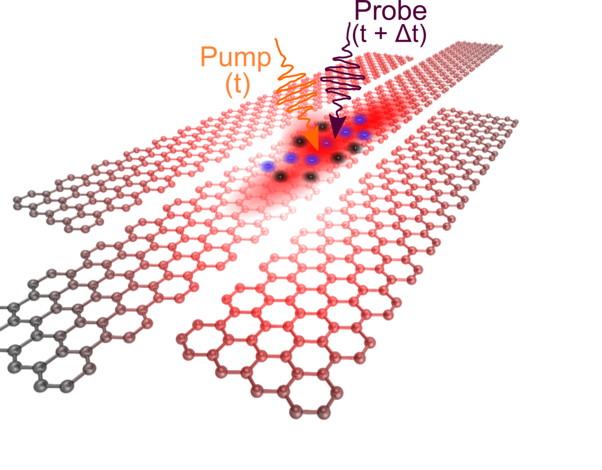
Following ultrafast charge flow in graphene nanoribbons

Collaborative paper published in Advanced Materials

Determining the electronic transport properties of graphene nanoribbons is crucial for assessing their suitability for applications. So far, this has been highly challenging both through experimental and theoretical approaches. This is particularly the case for graphene nanoribbons that are prepared by chemical vapor deposition, which is a scalable and industry-compatible bottom-up growth method that results in closely packed arrays of ribbons with relatively short lengths of a few tens of nanometers. In this study, the experimental technique of spatiotemporal microscopy is applied to study monolayer films of 9-armchair graphene nanoribbons prepared using this growth method, and combined with linear-scaling quantum transport calculations of arrays of thousands of nanoribbons. Both approaches directly resolve electronic spreading in space and time through diffusion and give an initial diffusivity approaching 200 cm2/s during the first picosecond after photoexcitation. This corresponds to a mobility up to 550 cm2/Vs. The quasi-free carriers then form excitons, which spread with a diffusivity of tens of cm2/s. The results indicate that this relatively large charge carrier mobility is the result of electronic transport not being hindered by defects nor inter-ribbon hopping. This confirms their suitability for applications that require efficient electronic transport.

Sebin successfully defends his PhD thesis; obtains cum laude

Congratulations, Sebin!

Thesis abstract:

It has been a longstanding goal of physicists to understand how heat flows and how it affects the thermal properties of materials. This quest has been driven not only by the pursuit of knowledge but also by the tremendous importance of heat in daily life. The discovery of new materials has introduced challenges in understanding fundamental properties such as heat transport, while also opening avenues for technological advancements.

In this thesis, we investigate the heat transport properties of a class of layered materials known as transition metal dichalcogenides (TMDs). We study these materials using two different optical techniques: the conventional technique of Raman thermometry and a novel spatiotemporal pump-probe thermometry technique that we have developed.

With this new technique, we directly quantify the in-plane thermal diffusivity in TMDs. The thermal diffusivities obtained for MoSe2, down to a thickness of 3 layers, are consistent with results obtained from Raman thermometry. Interestingly, in monolayer and bilayer samples, we observe a transition in heat transport behaviour—from diffusive in thicker samples to viscous with very low diffusivity in ultrathin samples. We attribute this viscous transport to the hydrodynamic flow of heat, a phenomenon that has never been observed in TMDs at any temperature.